Shenzhen Tengxingsheng Electronics Co., Ltd.
Contact: Miss Wen
Tel: 0755-23286182
Mob: 13570819121
QQ: 1456258664
QQ: 2316907424
Fax: 0755-23286183
Email: txspcbsc@163.com txspcb@163.com
Web : en.txspcb.cn
Add: 3rd Floor, Building 3, Jinkang Industrial Park, No. 1 Shajing Road, Baoan District, Shenzhen
Compared with single -sided circuit boards , double-sided circuit boards have higher wiring density and smaller apertures. The metallized holes on which the layer-to-layer interconnection depends are directly related to the reliability of the printed circuit board. With the reduction of the aperture, some debris, such as grinding debris, volcanic ash, etc., once left in the small hole, will make the electroless copper deposition and electroplating copper useless.
In order to ensure the reliable conduction effect of the double-sided circuit, the connection holes on the board should be welded with wires first, and the protruding part of the connection wire tip should be cut off to avoid hurting the operator's hand. This is the preparation work for the connection of the board. So, what problems should we pay attention to when welding double-sided circuit boards?
1. For devices that require shaping, they should be shaped first and then plugged in according to the requirements of the process drawings.
2. After shaping, the model side of the diode should face up, and there should be no difference in the length of the two pins.
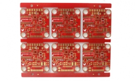
3. When inserting devices with polarity requirements, it should be noted that the polarity should not be reversed. After the device is inserted, whether it is vertical or horizontal, there should be no obvious tilt. PCB circuit board
4. The power of the soldering iron used for soldering is between 25 and 40W, the temperature of the soldering iron tip should be controlled at about 242°C, and the soldering time should be controlled within 3 to 4 seconds.
5. When welding, generally operate according to the principle of welding from short to high, and from the inside to the outside. The welding time should be mastered well. If the time is too long, the device will be scalded, and the copper-clad lines on the copper-clad laminate will also be scalded.
6. Because it is double-sided soldering, a process frame for placing the circuit board should also be made, so as not to slant the devices below.
7. After the welding is completed, a comprehensive inspection should be carried out to check the places where there are leaks and leaks. After confirmation, the excess device pins should be trimmed, and then flow into the next process.
8. The specific operation should also strictly follow the relevant process standards to ensure the welding quality. Industrial control PCB circuit board
The above are the precautions for the welding operation of double-sided circuit boards. If you don’t understand, you can consult Tengxingsheng at any time.

Mob: 13570819121
Email: txspcbsc@163.com
Web : www.txspcb.cn
Add: Jinkang, No. 1 Shajing Road, Baoan District, Shenzhen
3rd Floor, Building 3, Industrial Park

SWEEP